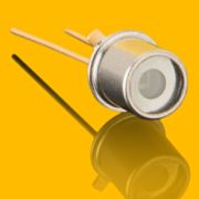
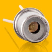
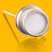
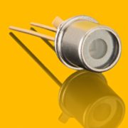
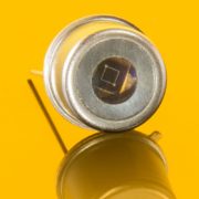
UVC
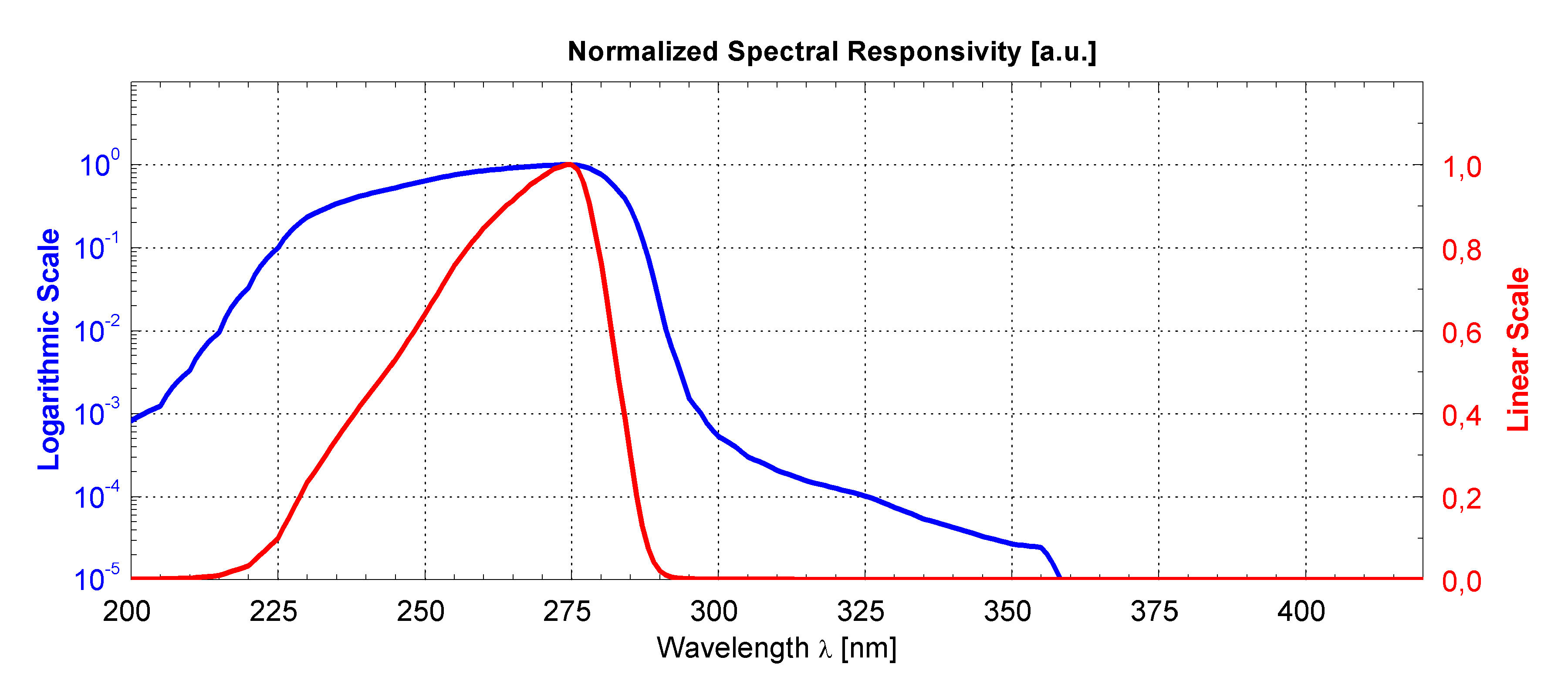
spectral sensitivity from 225 to 287 nm, peak wavelength 275 nm,
according to DVGW W 294-3:2006 and OENORM M5873 and DIN 19294,
special version to control UVC LED available, different packagings, sorted by increasing detector areas.
Showing all 22 results
-
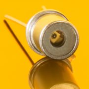
SG01S-C18
UVC, chip active area = 0.06 mm², TO18 housingProduct Description- UVC
- 0.06 mm2 detector area
- TO18 hermetically sealed metal housing, 1 isolated pin and 1 case pin
- 10 mW/cm2 irradiation at 275 nm (peak responsivity) results a current of approx. 960 nA
- SiC chip with PTB reported high radiation hardness
-

SG01S-C18-LED
UVC photodiode for UVC LED measurement, chip active area = 0.06 mm², TO18 housingProduct Description- UVC photodiode for UVC LED measurement
- 0.06 mm2 detector area
- TO18 hermetically sealed metal housing, 1 isolated pin and 1 case pin
- 10 mW/cm2 irradiation at 285 nm (peak responsivity) results a current of approx. 960 nA
- SiC chip with PTB reported high radiation hardness
-
SG01S-C18D
UVC, chip active area = 0.06 mm², with diffuser, TO18 housingProduct Description- UVC
- 0.06 mm2 detector area
- uses a diffuser to produce a Lambertian response over the aperture
- TO18 hermetically sealed metal housing, 1 isolated pin and 1 case pin
- 10 mW/cm2 irradiation at 275 nm (peak responsivity) results a current of approx. 116 nA
- SiC chip with PTB reported high radiation hardness
-
SG01S-C18ISO90
UVC, chip active area = 0.06 mm², TO18 housing, isolatedProduct Description- UVC
- 0.06 mm2 detector area
- TO18 hermetically sealed metal housing, two isolated pins, one additional grounded pin
- 10 mW/cm2 irradiation at 275 nm (peak responsivity) results a current of approx. 960 nA
- SiC chip with PTB reported high radiation hardness
-
SG01S-C18ISO90D
UVC, chip active area = 0.06 mm², with diffuser, TO18 housing, isolatedProduct Description- UVC
- 0.06 mm2 detector area
- uses a diffuser to produce a Lambertian response over the aperture
- TO18 hermetically sealed metal housing, two isolated pins, one additional grounded pin
- 10 mW/cm2 irradiation at 275 nm (peak responsivity) results a current of approx. 116 nA
- SiC chip with PTB reported high radiation hardness
-
SG01S-C5
UVC, chip active area = 0.06 mm², TO5 housingProduct Description- UVC
- 0.06 mm2 detector area
- TO5 hermetically sealed metal housing, 1 isolated pin and 1 case pin
- 10 mW/cm2 irradiation at 275 nm (peak responsivity) results a current of approx. 960 nA
- SiC chip with PTB reported high radiation hardness
-
SG01M-C18
UVC, chip active area = 0.20 mm², TO18 housingProduct Description- UVC
- 0.20 mm2 detector area
- TO5 hermetically sealed metal housing, 1 isolated pin and 1 case pin
- 10 mW/cm2 irradiation at 275 nm (peak responsivity) results a current of approx. 3200 nA
- SiC chip with PTB reported high radiation hardness
-
SG01M-C18ISO90
UVC, chip active area = 0.20 mm², TO18 housing, isolatedProduct Description- UVC
- 0.20 mm2 detector area
- TO18 hermetically sealed metal housing, two isolated pins, one additional grounded pin
- 10 mW/cm2 irradiation at 275 nm (peak responsivity) results a current of approx. 3200 nA
- SiC chip with PTB reported high radiation hardness
-
SG01M-C5
UVC, chip active area = 0.20 mm², TO5 housingProduct Description- UVC
- 0.20 mm2 detector area
- TO5 hermetically sealed metal housing, 1 isolated pin and 1 case pin
- 10 mW/cm2 irradiation at 275 nm (peak responsivity) results a current of approx. 3200 nA
- SiC chip with PTB reported high radiation hardness
-
SG01M-C5ISO90
UVC, chip active area = 0.20 mm², TO5 housing, isolatedProduct Description- UVC
- 0.20 mm2 detector area
- TO5 hermetically sealed metal housing, two isolated pins, one additional grounded pin
- 10 mW/cm2 irradiation at 275 nm (peak responsivity) results a current of approx. 3200 nA
- SiC chip with PTB reported high radiation hardness
-
SG01M-C5D
UVC, chip active area = 0.20 mm², with diffuser, TO5 housingProduct Description- UVC
- 0.20 mm2 detector area
- uses a diffuser to produce a Lambertian response over the aperture
- TO5 hermetically sealed metal housing, 1 isolated pin and 1 case pin
- 10 mW/cm2 irradiation at 275 nm (peak responsivity) results a current of approx. 420 nA
- SiC chip with PTB reported high radiation hardness
-
SG01D-C18
UVC, chip active area = 0.50 mm², TO18 housingProduct Description- UVC
- 0.50 mm2 detector area
- TO18 hermetically sealed metal housing, 1 isolated pin and 1 case pin
- 10 µW/cm2 irradiation at 275 nm (peak responsivity) results a current of approx. 8 nA
- SiC chip with PTB reported high radiation hardness
-
SG01D-C18ISO90
UVC, chip active area = 0.50 mm², TO18 housing, isolatedProduct Description- UVC
- 0.50 mm2 detector area
- TO18 hermetically sealed metal housing, two isolated pins, one additional grounded pin
- 10 µW/cm2 irradiation at 275 nm (peak responsivity) results a current of approx. 8 nA
- SiC chip with PTB reported high radiation hardness
-
SG01D-C18D
UVC, chip active area = 0.5 mm², with diffuser, TO18 housingProduct Description- UVC
- 0.5 mm2 detector area
- uses a diffuser to produce a Lambertian response over the aperture
- TO18 hermetically sealed metal housing, 1 isolated pin and 1 case pin
- 10 µW/cm2 irradiation at 275 nm (peak responsivity) results a current of approx. 0.9 nA
- SiC chip with PTB reported high radiation hardness
-
SG01D-C5ISO90
UVC, chip active area = 0.50 mm², TO5 housing, isolatedProduct Description- UVC
- 0.50 mm2 detector area
- TO5 hermetically sealed metal housing, two isolated pins, one additional grounded pin
- 10 µW/cm2 irradiation at 275 nm (peak responsivity) results a current of approx. 8 nA
- SiC chip with PTB reported high radiation hardness
-
SG01D-C5Lens
UVC, chip active area = 0.50 mm², TO5 lens capProduct Description- UVC
- 0.50 mm² detector area
- TO5 hermetically sealed metal housing with concentrating lens
- 10 µW/cm² irradiation at 275 nm (peak responsivity) results a current of approx. 42 nA
- 1 isolated pin and 1 case pin
- SiC chip with PTB reported high radiation hardness
-
SG01D-C5D
UVC, chip active area = 0.50 mm², with diffuser, TO5 housingProduct Description- UVC
- 0.50 mm2 detector area
- uses a diffuser to produce a Lambertian response over the aperture
- TO5 hermetically sealed metal housing, 1 isolated pin and 1 case pin
- 10 µW/cm2 irradiation at 275 nm (peak responsivity) results a current of approx. 0.9 nA
- SiC chip with PTB reported high radiation hardness
-
SG01L-C18
UVC, chip active area = 1.00 mm², TO18 housingProduct Description- UVC
- 1.00 mm2 detector area
- TO5 hermetically sealed metal housing, 1 isolated pin and 1 case pin
- 10 µW/cm2 irradiation at 275 nm (peak responsivity) results a current of approx. 16 nA
- SiC chip with PTB reported high radiation hardness
-
SG01L-C5
UVC, chip active area = 1.00 mm², TO5 housingProduct Description- UVC
- 1.00 mm2 detector area
- TO5 hermetically sealed metal housing, 1 isolated pin and 1 case pin
- 10 µW/cm2 irradiation at 275 nm (peak responsivity) results a current of approx. 16 nA
- SiC chip with PTB reported high radiation hardness
-
SG01L-C5D
UVC, chip active area = 1.00 mm², with diffuser, TO5 housingProduct Description- UVC
- 1.00 mm2 detector area
- uses a diffuser to produce a Lambertian response over the aperture
- TO5 hermetically sealed metal housing, 1 isolated pin and 1 case pin
- 10 µW/cm2 irradiation at 275 nm (peak responsivity) results a current of approx. 2 nA
- SiC chip with PTB reported high radiation hardness
-
SG01F-C5
UVC, chip active area = 1.82 mm², TO5 housingProduct Description- UVC
- 1.82 mm2 detector area
- TO5 hermetically sealed metal housing, 1 isolated pin and 1 case pin
- 1 µW/cm2 irradiation at 275 nm (peak responsivity) results a current of approx. 3 nA
- SiC chip with PTB reported high radiation hardness
-
SG01XL-C5
UVC, chip active area = 7.60 mm², TO5 housingProduct Description- UVC
- 7.60 mm2 detector area
- TO5 hermetically sealed metal housing, 1 isolated pin and 1 case pin
- 10 µW/cm2 irradiation at 275 nm (peak responsivity) results a current of approx. 120 nA
- SiC chip with PTB reported high radiation hardness


