
UV Photodiodes
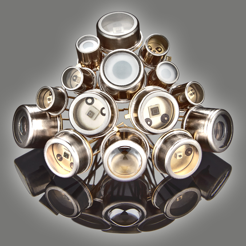
- active area from 0.06 mm² to 36 mm² and quadrant photodiodes for position detections
- spectral response for broadband UV or filtered for UVA, UVB, UVC or UV-Index
- various entrance optics and housings options available (TO or SMD)
- our own SiC photodiode chip production since 2009
- also available with VUV sensitivity
- PTB (German equivalent of NIST or NPL) measured high radiation hardness
- 350°C high temperature stable photodiodes available
- photodiode application guide
All photodiodes are always on stock, no minimum order quantity. They can be ordered via our web shop or with an email addressed to welcome@sglux.de or from DigiKey. Alternatively, we are happy to issue a quotation or you may click on our shop’s QUOTATION function, instead of CHECKOUT.
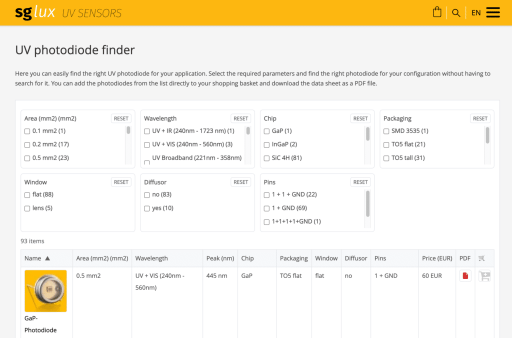
We also offer the option of finding photodiodes directly for your application using a product finder with parameter filters.
Showing 31–60 of 91 results
-

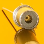
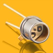
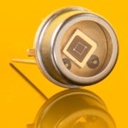
SG01D-B5
UVB, chip active area = 0.50 mm², TO5 housingProduct Description- UVB
- 0.50 mm2 detector area
- TO5 hermetically sealed metal housing, 1 isolated pin and 1 case pin
- 10 µW/cm2 irradiation at 310 nm (peak responsivity) results a current of approx. 1 nA
- SiC chip with PTB reported high radiation hardness
-
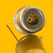
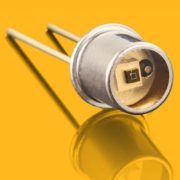
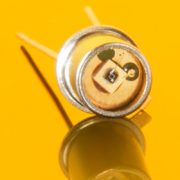
SG01L-BC18
UVB+UVC, chip active area = 1.00 mm², TO18 housingProduct Description- UVB+UVC
- 1.00 mm2 detector area
- TO18 hermetically sealed metal housing, 1 isolated pin and 1 case pin
- 10 µW/cm2 irradiation at 280 nm (peak responsivity) results a current of approx. 17 nA
- SiC chip with PTB reported high radiation hardness
-
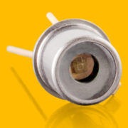
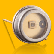
SG01L-BC5
UVB+UVC, chip active area = 1.00 mm², TO5 housingProduct Description- UVB+UVC
- 1.00 mm2 detector area
- TO5 hermetically sealed metal housing, 1 isolated pin and 1 case pin
- 10 µW/cm2 irradiation at 280 nm (peak responsivity) results a current of approx. 17 nA
- SiC chip with PTB reported high radiation hardness
-

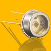
SG01XL-BC5
UVB+UVC, chip active area = 7.60 mm², TO5 housingProduct Description- UVB+UVC
- 7.60 mm2 detector area
- TO5 hermetically sealed metal housing, 1 isolated pin and 1 case pin
- 10 µW/cm2 irradiation at 280 nm (peak responsivity) results a current of approx. 122 nA
- SiC chip with PTB reported high radiation hardness
-
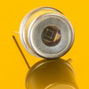
SG01S-A18
UVA, chip active area = 0.06 mm², TO18 housingProduct Description- UVA
- 0.06 mm2 detector area
- TO18 hermetically sealed metal housing, 1 isolated pin and 1 case pin
- 10 mW/cm2 irradiation at 331 nm (peak responsivity) results a current of approx. 273 nA
- SiC chip with PTB reported high radiation hardness
-

SG01S-A5
UVA, chip active area = 0.06 mm², TO5 housingProduct Description- UVA
- 0.06 mm2 detector area
- TO5 hermetically sealed metal housing, 1 isolated pin and 1 case pin
- 10 mW/cm2 irradiation at 331 nm (peak responsivity) results a current of approx. 273 nA
- SiC chip with PTB reported high radiation hardness
-

SG01M-A18
UVA, chip active area = 0.20 mm², TO18 housingProduct Description- UVA
- 0.20 mm2 detector area
- TO18 hermetically sealed metal housing, 1 isolated pin and 1 case pin
- 10 mW/cm2 irradiation at 331 nm (peak responsivity) results a current of approx. 910 nA
- SiC chip with PTB reported high radiation hardness
-
SG01M-A5
UVA, chip active area = 0.20 mm², TO5 housingProduct Description- UVA
- 0.20 mm2 detector area
- TO5 hermetically sealed metal housing, 1 isolated pin and 1 case pin
- 10 mW/cm2 irradiation at 331 nm (peak responsivity) results a current of approx. 910 nA
- SiC chip with PTB reported high radiation hardness
-
SG01D-A18
UVA, chip active area = 0.50 mm², TO18 housingProduct Description- UVA
- 0.50 mm2 detector area
- TO18 hermetically sealed metal housing, 1 isolated pin and 1 case pin
- 10 µW/cm2 irradiation at 331 nm (peak responsivity) results a current of approx. 2.27 nA
- SiC chip with PTB reported high radiation hardness
-
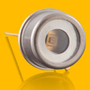
SG01D-A18ISO90
UVA, chip active area = 0.50 mm², TO18 housing, isolatedProduct Description- UVA
- 0.50 mm2 detector area
- TO18 hermetically sealed metal housing, two isolated pins, one additional grounded pin
- 10 µW/cm2 irradiation at 331 nm (peak responsivity) results a current of approx. 2.3 nA
- SiC chip with PTB reported high radiation hardness
-
SG01D-A5
UVA, chip active area = 0.50 mm², TO5 housingProduct Description- UVA
- 0.50 mm2 detector area
- TO5 hermetically sealed metal housing, 1 isolated pin and 1 case pin
- 10 µW/cm2 irradiation at 331 nm (peak responsivity) results a current of approx. 2.3 nA
- SiC chip with PTB reported high radiation hardness
-

SG01L-A18
UVA, chip active area = 1.00 mm², TO18 housingProduct Description- UVA
- 1.00 mm2 detector area
- TO18 hermetically sealed metal housing, 1 isolated pin and 1 case pin
- 10 µW/cm2 irradiation at 331 nm (peak responsivity) results a current of approx. 4.6 nA
- SiC chip with PTB reported high radiation hardness
-

SG01L-A5
UVA, chip active area = 1.00 mm², TO5 housingProduct Description- UVA
- 1.00 mm2 detector area
- TO5 hermetically sealed metal housing, 1 isolated pin and 1 case pin
- 10 µW/cm2 irradiation at 331 nm (peak responsivity) results a current of approx. 4.6 nA
- SiC chip with PTB reported high radiation hardness
-
SG01XL-A5
UVA, chip active area = 7.60 mm², TO5 housingProduct Description- UVA
- 7.60 mm2 detector area
- TO5 hermetically sealed metal housing, 1 isolated pin and 1 case pin
- 10 µW/cm2 irradiation at 331 nm (peak responsivity) results a current of approx. 34 nA
- SiC chip with PTB reported high radiation hardness
-
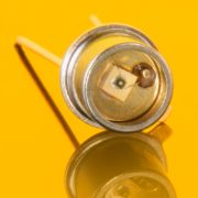
SG01S-18
UVA+UVB+UVC, chip active area = 0.06 mm², TO18 housingProduct Description- UV broadband (UVA+UVB+UVC)
- 0.06 mm² detector area
- TO18 hermetically sealed metal housing, 1 isolated pin and 1 case pin
- 10 mW/cm² irradiation at 280 nm (peak responsivity) results a current of approx. 960 nA
- SiC chip with PTB reported high radiation hardness
-
SG01S-18S
UVA+UVB+UVC, chip active area = 0.06 mm², TO18 short capProduct Description- UV broadband (UVA+UVB+UVC)
- 0.06 mm2 detector area
- flat TO18 hermetically sealed metal housing, 1 isolated pin and 1 case pin
- 10 mW/cm2 irradiation at 280 nm (peak responsivity) results a current of approx. 960 nA
- SiC chip with PTB reported high radiation hardness
-
SG01S-18ISO90
UVA+UVB+UVC, chip active area = 0.06 mm², TO18 housing, isolatedProduct Description- UV broadband (UVA+UVB+UVC)
- 0.06 mm² detector area
- TO18 hermetically sealed metal housing, two isolated pins, one additional grounded pin
- 10 mW/cm² irradiation at 280 nm (peak responsivity) results a current of approx. 960 nA
- SiC chip with PTB reported high radiation hardness
-

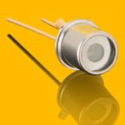
SG01S-18D
UVA+UVB+UVC, chip active area = 0.06 mm², with diffuser, TO18 housingProduct Description- UV broadband (UVA+UVB+UVC)
- 0.06 mm² detector area
- uses a diffuser to produce a Lambertian response over the aperture
- TO18 hermetically sealed metal housing, 1 isolated pin and 1 case pin
- 10 mW/cm² irradiation at 280 nm (peak responsivity) results a current of approx. 123 nA
- SiC chip with PTB reported high radiation hardness
-

SG01S-5
UVA+UVB+UVC, chip active area = 0.06 mm², TO5 short capProduct Description- UV broadband (UVA+UVB+UVC)
- 0.06 mm² detector area
- flat TO5 hermetically sealed metal housing, 1 isolated pin and 1 case pin
- 10mW/cm² irradiation at 280nm (peak responsivity) results a current of approx. 960 nA
- SiC chip with PTB reported high radiation hardness
-
SG03R05-18
UVA+UVB+UVC+VUV, chip active area = 0.5 mm², TO18 capProduct Description- UV broadband (UVA+UVB+UVC+VUV)
- 0.5 mm² detector area
- TO18 hermetically sealed metal housing, 1 isolated pin and 1 case pin
- 10mW/cm² irradiation at 280nm (peak responsivity) results a current of approx. 8 µA
-
SG03R05-5
UVA+UVB+UVC+VUV, chip active area = 0.5 mm², TO5 short capProduct Description- UV broadband (UVA+UVB+UVC+VUV)
- 0.5 mm² detector area
- flat TO5 hermetically sealed metal housing, 1 isolated pin and 1 case pin
- 10mW/cm² irradiation at 280nm (peak responsivity) results a current of approx. 8 µA
- wide FOV
-

SG03R10-5
UVA+UVB+UVC+VUV, chip active area = 1.0 mm², TO5 short capProduct Description- UV broadband (UVA+UVB+UVC)
- 1.0 mm² detector area
- flat TO5 hermetically sealed metal housing, 1 isolated pin and 1 case pin
- 10µW/cm² irradiation at 280nm (peak responsivity) results a current of approx. 16 nA
- wide FOV
-
SG03R20-5
UVA+UVB+UVC+VUV, chip active area = 2.0 mm², TO5 short capProduct Description- UV broadband (UVA+UVB+UVC+VUV)
- 2.0 mm² detector area
- flat TO5 hermetically sealed metal housing, 1 isolated pin and 1 case pin
- 10µW/cm² irradiation at 280nm (peak responsivity) results a current of approx. 32 nA
- wide FOV
-
SG03R20-5_MgF
UVA+UVB+UVC+VUV up to 120 nm, chip active area = 2.0 mm², TO5 short capProduct Description- UV broadband (UVA+UVB+UVC+VUV up to 120nm)
- 2.0 mm² detector area
- flat TO5 hermetically sealed metal housing, 1 isolated pin and 1 case pin
- 10µW/cm² irradiation at 280nm (peak responsivity) results a current of approx. 32 nA
- wide FOV
-
SG03R80-5
UVA+UVB+UVC+VUV, chip active area = 8.0 mm², TO5 short capProduct Description- UV broadband (UVA+UVB+UVC+VUV)
- 8.0 mm² detector area
- flat TO5 hermetically sealed metal housing, 1 isolated pin and 1 case pin
- 1µW/cm² irradiation at 280nm (peak responsivity) results a current of approx. 13 nA
- wide FOV
-
SG03R01-5
UVA+UVB+UVC+VUV, chip active area = 0.1 mm², TO5 short capProduct Description- UV broadband + VUV responsivity (UVA+UVB+UVC+VUV)
- 0.1 mm² detector area
- flat TO5 hermetically sealed metal housing, 1 isolated pin and 1 case pin
- 10mW/cm² irradiation at 280nm (peak responsivity) results a current of approx. 1600nA
-
SG01M-18
UVA+UVB+UVC, chip active area = 0.20 mm², TO18 housingProduct Description- UV broadband (UVA+UVB+UVC)
- 0.20 mm² detector area
- TO18 hermetically sealed metal housing, 1 isolated pin and 1 case pin
- 10mW/cm² irradiation at 280 nm (peak responsivity) results a current of approx. 3200 nA
- SiC chip with PTB reported high radiation hardness
-
SG01M-18S
UVA+UVB+UVC, chip active area = 0.20 mm², TO18 short capProduct Description- UV broadband (UVA+UVB+UVC)
- 0.20 mm2 detector area
- flat TO18 hermetically sealed metal housing, 1 isolated pin and 1 case pin
- 10mW/cm2 irradiation at 280 nm (peak responsivity) results a current of approx. 3200 nA
- SiC chip with PTB reported high radiation hardness
-
SG01M-18ISO90
UVA+UVB+UVC, chip active area = 0.20 mm², TO18 housing, isolatedProduct Description- UV broadband (UVA+UVB+UVC)
- 0.20 mm² detector area
- TO18 hermetically sealed metal housing, two isolated pins, one additional grounded pin
- 10 mW/cm² irradiation at 280 nm (peak responsivity) results a current of approx. 3200 nA
- SiC chip with PTB reported high radiation hardness
-
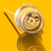
SG01M6H-18
UVA+UVB+UVC, 6H SiC chip, chip active area = 0.20 mm², TO18 housingProduct Description- UV broadband (UVA+UVB+UVC)
- 6H SiC chip for enhanced UV sensitivity, e.g. UVA LED control
- 0.20 mm² detector area
- TO18 hermetically sealed metal housing, 1 isolated pin and 1 case pin
- 10mW/cm² irradiation at 290 nm (peak responsivity) results a current of approx. 3200 nA