sglux – house of photodiodes – from 120nm to 1700nm
Customized special designs from vacuum UV to infrared
sglux has established itself as a well-known brand for SiC photodiodes and sensors worldwide. Going this path, sglux has ventured into designing of customer-specific photodiodes, becoming a one-stop agency for all measurement requirements in the wavelength range from vacuum UV to infrared radiation. These can incorporate one or more chips, filters and optics, SiO₂ diffusers or VUV-transparent MgF based windows.
Our offering
• Application-specific design of detectors or assemblies based on SiC, GaP, InGaP, InGaAs, Si, Ge, or any other material suitable for the application
• Use of commercially available optical filters, diffusers, and lenses, as well as in-house development if these are not available on the market.
• Integration of temperature sensors
• Circuit development for processing photocurrents (often only a few nA) into standard process variables, such as 0-5V, 4-20mA, or digital, for use in photodiode housings (sglux TOCONs) or outside
• Assembly and connection technology
• Development of special housings
Our strengths
• We enjoy implementing special concepts and have over 20 years of experience in building complex detectors with or without amplifiers, with or without filters, with one or more different chips, always with the highest possible precision and long-term stability.
• In-house production of SiC photodiode chips in three variants: standard, VUV, and APD, as well as the production of InGaP photodiode chips.
• Extensive experience in working with other chips, such as GaP, InGaAs, Si, Ge.
• High-performance calibration laboratory with first-class equipment, constant exchange with the PTB, regular “round robins” with other leading suppliers in Germany for quality assurance, participation in various standardization committees.
Showing the single result
-

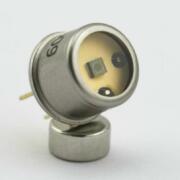
SG01-TANDEM-XL
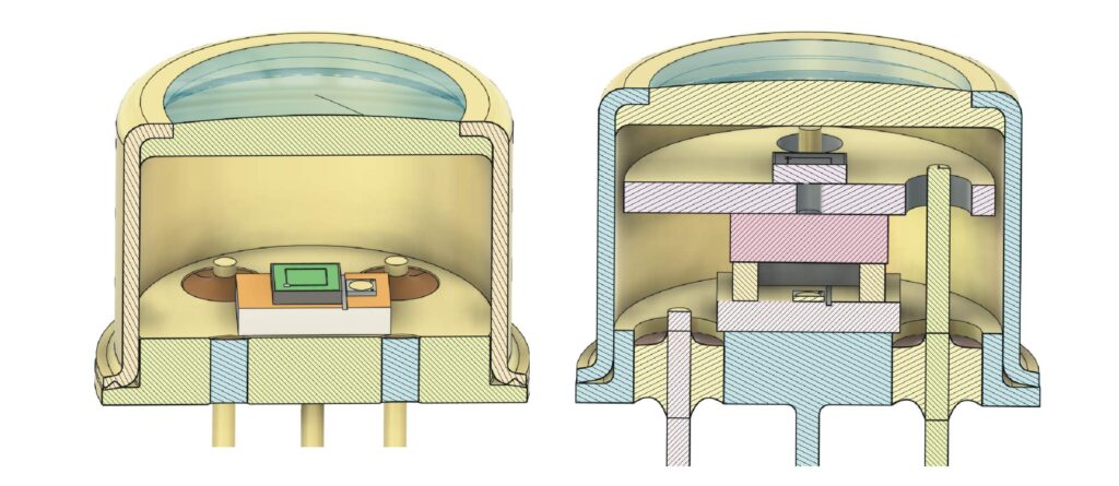
UVA+IR, active area UV chip = 7.60mm², active area InGaAs chip = 7.07mm², TO5 cap, for flame monitoring applications, other models can be produced, e.g. with a smaller SiC chip (1.82mm²) to save costs or with chips arranged next to each other instead of on top of each other. The advantage of this arrangement is a further further cost savings, the disadvantage is increased focusing effort. The IR sensor can be equipped with filters, e.g. to suppress visible radiation on the measured value.Product Description- Double-chip photodiodes for simultaneous measurement of UV and IR
- active area UV chip = 7.60mm²
- active area InGaAs chip = 7.07mm²
- TO5 housing hermetically encapsulated with 4 isolated pins
- further models can be produced, e.g. with a smaller SiC chip (1.82mm2) to save costs
- models available with chips arranged next to each other instead of on top of each other
- option of equipping the IR sensor with additional filters, e.g. to suppress visible radiation on the measured value